-
For PR Teams
For PR Teams
Overview
Use Cases
Capabilities
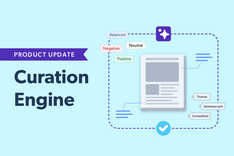
Introducing Curation Engine
A new AI capability that delivers analysis-ready Media Intelligence. More than just a product launch, this is a shift in how communications teams monitor, understand and act on media coverage.
Learn more - For Journalists
-
Resources
Resources
Commmunity
Customers
- Pricing
-
Company
Company
- Log In
- Request Demo